|
|
|
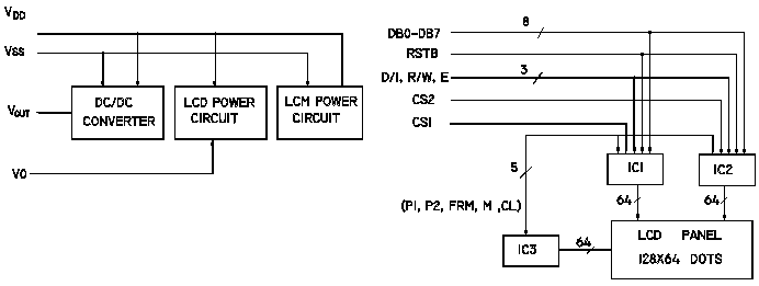
1 Outline dimensions2 Block diagram
3 Mechanical specification
| Item | Specifications | Unit |
| Dimensinal Outline | 93.0(W)ˇÁ70.0(H)ˇÁ13.0 MAX.(T) | mm |
| View Area | 71.7(W)ˇÁ39.0(H) | mm |
| Effective V/Area | 66.52(W)ˇÁ33.24(H) | mm |
| Dots ˇÁ Dots | 128ˇÁ64 Dots | -- |
| Dot Pitch | 0.52(W)ˇÁ0.52(H ) | mm |
| Dot Size | 0.48(W)ˇÁ0.48(H) | mm |
4 ABSOLUTE MAXIMUM RATINGS
| Item | Symbol | Test Condition |
Standard Value
|
Unit
|
|
|
Min.
|
Max.
|
||||
| Supply Voltage for Logic | Vdd-Vss |
Ta=25oC
|
-0.3
|
7.0
|
V
|
| Supply Voltage for LCD | Vo |
Vdd-19.0
|
Vdd+0.3
|
V
|
|
| Input Voltage | Vi |
-0.3
|
Vdd-0.3
|
V
|
|
| Operating Temperature | Topr |
-
|
-20
|
70
|
oC
|
| Storage Temperature | Tstg |
-
|
-30
|
80
|
oC
|
5 ELECTRICAL CHARACTERISTICS (Ta=25oC)
| Item | Symbol | Test Condition |
Standard Value
|
Unit | |||
|
Min.
|
Typ.
|
Max.
|
|||||
| Supply Voltage for Logic | Vdd-Vss |
-
|
4.5
|
-
|
5.5
|
V
|
|
| Supply Current for | Logic |
Idd
|
IOH = 0.2mA
|
-
|
10.0
|
15.0
|
mA
|
| LCD |
-
|
IOL = 1.2mA
|
-
|
mA
|
|||
| Operating Voltage for LCD | Vdd-Vo |
-
|
-
|
-
|
-
|
V
|
|
|
Ta=25oC
|
-
|
12.5 |
-
|
V
|
|||
|
-
|
-
|
-
|
-
|
V
|
|||
| Input Voltage | "H"Level | VIH |
High Level
|
0.7Vdd
|
-
|
Vdd
|
V
|
| "L"Level | VIL |
Low Level
|
0
|
-
|
0.3Vdd
|
V
|
|
6 INTERFACE PIN CONNECTIONS
| PIN NO. | SYMBOL | LEVEL | FUNCTION |
| Vss |
0V
|
Power supply(GND) | |
| Vdd |
5.0V
|
Power supply | |
| Vo |
-
|
Contrast Adjust | |
| D/I |
H/L
|
H: Display data L: Instruction code | |
| R/W |
H/L
|
H: Data/status read L: Data/instruction write | |
| E |
H,H/L
|
Chip enable signal | |
| 7 - 14 | DB0 - DB7 |
H/L
|
Data bus line |
| CS1 |
H
|
Chip selection for IC1 | |
| CS2 |
H
|
Chip selection for IC2 | |
| RST |
L
|
Reset Signal | |
| Vout |
-
|
Negativ Voltage Output | |
| LED+ |
-
|
Power Supply for LED Back Light + | |
| LED- |
-
|
Power Supply for LED Back Light - | |